
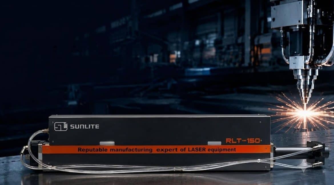
You might see crude welding sparks in large auto factories. Then, you might think CO2 lasers are outdated. Nevertheless, in cleanroom labs, a 10.6-micrometer (μm) infrared light persists. This light is a “stabilizing anchor” for precise silicon chips. It also handles complex semiconductor materials. The high-power Slab CO2 RF laser is essential here.
I. The Unique Beauty of “Slab”: The Mystery of Diffusion Cooling
High-power kilowatt-class CO2 lasers face a core challenge: heat dissipation. Conventional convective airflow cooling creates turbulence. This makes the laser beam unstable. Its quality suffers. Leading manufacturers, like Yongli, use a Slab CO2 RF laser design. This cleverly resolves the issue. This advanced Slab CO2 RF laser technology relies on diffusion cooling. Imagine laser gas. It is thinly sandwiched between two high-precision metal plates. The gas layer is extremely thin. Heat from the discharge quickly diffuses outward. It passes through the metal plate walls.
This design offers brilliant advantages:
- Static Cavity: It requires no strong airflow circulation. The laser cavity remains quiet and stable.
- Excellent Waveguide Effect: The narrow gap between metal plates naturally confines the beam. It effectively filters higher-order noise modes. This ensures a near-perfect fundamental mode distribution. The Slab CO2 RF laser achieves superior beam quality.
II. Why Is It “Irreplaceable”?
You might ask: Why does high-end IC manufacturing still use a high-power Slab CO2 RF laser? Fiber lasers are faster and cheaper.
- Wavelength is Critical: Fiber lasers operate around 1.06 μm. CO2 lasers use 10.6 μm. Many semiconductor materials (like photoresists, polymers, ceramics) strongly absorb the 10 μm band. A fiber laser might just scorch these surfaces. In contrast, a CO2 laser achieves precise, clean, molecular vaporization. This prevents thermal damage.
- Gentle Annealing for Silicon: For chip annealing, the high-power Slab CO2 RF laser offers distinct benefits. It provides extremely uniform energy coverage. It precisely controls wafer temperature gradients in short bursts. This effectively repairs lattice defects. Crucially, it avoids damage to delicate chip structures. This ultimate temperature field control remains unparalleled by other lasers.
III. Technical Challenges: The Threshold of Top-Tier Craftsmanship
Despite its excellent performance, the Slab CO2 RF laser faces strict technical challenges.
- Optical Mirrors Under Extreme Stress: Kilowatt laser power causes beams to oscillate between mirrors. Even minute impurities (parts per million) on a mirror surface absorb heat. This creates irreversible “thermal lensing distortion.” Beam quality suffers significantly. Thus, optical system material selection and coating represent the highest industry standards.
- RF Power Supply Synergy: The RF power supply delivers kilowatt-level energy. It must ensure extremely stable impedance matching at high frequencies. Tiny current or voltage fluctuations cause “pulse jitter” in the laser output. This directly impacts wafer annealing uniformity. Consequently, final quality also suffers.
IV. Outlook: The Future of a Heavy Sniper
Engineers demand extreme precision and specialized processes. They will not abandon the Slab CO2 RF laser for fiber lasers. Instead, its excellent stability, focused energy, and unique wavelength make it indispensable. It is a true “killer app” for process development.
The Slab CO2 RF laser remains irreplaceable. This applies to semiconductor packaging/testing, flexible circuit board processing, and high-end medical device micro-nano fabrication. It does not prioritize speed. Rather, it showcases modern engineering’s ultimate craftsmanship. It delivers profound strength in every micron of processing precision.
Therefore, when assessing a high-power Slab CO2 RF laser system, look beyond power. Focus on energy distribution stability. Also, consider its wavelength locking accuracy.