Microelectronic manufacturing deals with incredibly fine structures daily. Indeed, circuit boards are now paper-thin and silk-soft. Consequently, traditional mechanical punching or standard laser cutting methods often prove too aggressive. This frequently causes damage. However, RF-excited CO2 lasers truly excel. They offer precise control and inflict minimal damage. Therefore, RF laser technology fundamentally changes production. It innovates everything from basic depaneling to complex material processing.
I. Why Does Microelectronics Favor RF Lasers?
Indeed, heat is microelectronics processing’s greatest adversary. Traditional DC glass tube lasers respond slowly. Their beam switching often resembles slow baking delicate silk. This frequently leads to edge melting or charring. In stark contrast, RF lasers offer a key advantage: extremely high pulse frequency and rapid response. They switch on and off in mere nanoseconds. Therefore, RF laser energy bursts quickly, performs its task, and then immediately shuts down. This rapid “in-and-out” action, furthermore, minimizes the Heat Affected Zone (HAZ). Materials simply lack time to transfer heat to surrounding areas. Processing thus concludes swiftly. This nearly “cold processing” effect is crucial. Ultimately, it ensures high performance and stability for microelectronic components.
II. FPC Flexible Circuit Boards: The Perfect RF Laser “Tailor”
Flexible Printed Circuits (FPCs) are essential for modern foldable phones and ultra-thin laptops. These boards, moreover, comprise polyimide (PI) film layered with copper foil. Significantly, FPCs are extremely heat-sensitive. For FPC profile cutting, RF lasers (specifically 9.3µm wavelength models) demonstrate remarkable adaptability. PI material, notably, absorbs this particular wavelength very efficiently. Consequently, the RF laser cuts like a hot knife through butter. It consistently creates perfectly smooth, carbonization-free, and burr-free edges. Crucially, this process does not damage the underlying micron-sized copper lines. Therefore, it ensures complete circuit conductivity.
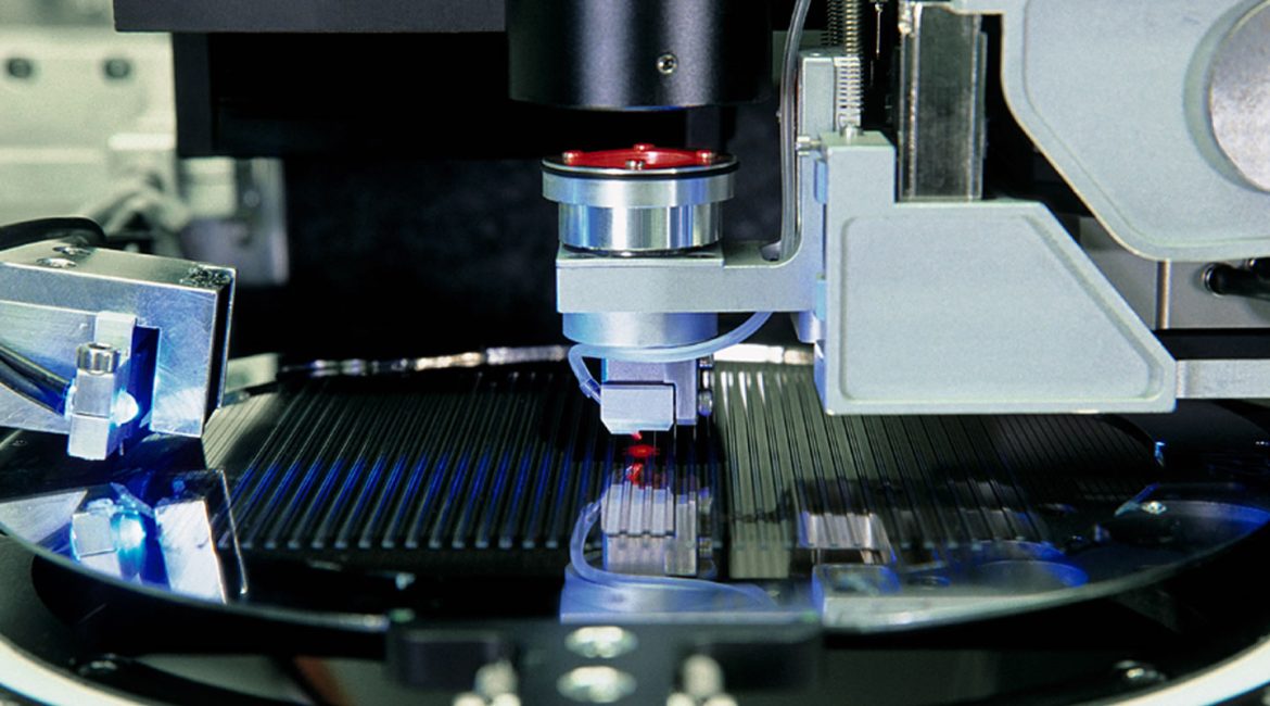
III. Precise Coverlayer Stripping and Residue Removal
PCB manufacturing always involves a protective coverlayer on the circuit surface. Before component assembly, we must precisely strip specific coverlayer areas. This action, naturally, exposes the underlying solder pads.
- Precise Stripping: RF lasers offer precise control over stripping depth. They rapidly vaporize the polymer coverlayer. Importantly, their action automatically halts or significantly weakens upon contacting the highly reflective copper layer. This “selective absorption” thus ensures clean exposure of solder pads.
- Residue Removal (De-gassing/De-smearing): Drilling or stripping operations often leave behind trace adhesives or organic debris. However, RF laser’s high-energy pulses instantly vaporize and remove these “smears.” This physical removal method is, furthermore, more environmentally friendly than chemical cleaning. Moreover, it integrates easily into fully automated production lines, boosting efficiency.
IV. PCB Depaneling and Stress Elimination: Ensuring Circuit Board Safety
Traditional mechanical milling cutters, unfortunately, introduce physical stress during PCB depaneling. This stress can cause desoldering of tiny surface-mount components. It may also lead to invisible internal cracks. In stark contrast, RF laser depaneling offers a non-contact solution. The RF laser beam directly vaporizes the substrate. It generates no mechanical pressure whatsoever. Consequently, this processing method provides the highest safety level. This applies especially to high-density multilayer boards or finished boards with expensive integrated chips. Furthermore, for precise scribing and stripping of PCB surface coverlayers, RF lasers guarantee no delamination or warping. This further safeguards product quality.
Summary: RF Lasers, The Unsung Heroes of Microelectronics Manufacturing
From precise FPC cutting to clean coverlayer processing, and then to stress-free depaneling of finished PCBs, RF lasers are fundamentally reshaping microelectronics production. They boast high frequency, minimal thermal impact, and long operational lifetimes. Consequently, RF laser technology significantly boosts product first-pass yield. More importantly, it enables unprecedented possibilities for electronic designs. These designs often pursue extreme thinness and ultimate performance. Undoubtedly, RF lasers serve as indispensable, often “invisible” heroes in modern microelectronics manufacturing.