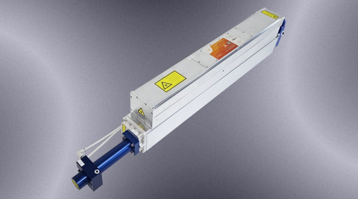
In the laser family, the high-power Slab CO2 RF laser stands as a hidden technological giant. Unlike traditional cylindrical glass tubes, it features a unique flat structure. Consequently, this Slab CO2 RF laser has carved out a premium niche in kilowatt (kW) and higher power applications.
I. Unique “Flat” Structure and the Secret of Diffusive Cooling
The most striking feature of a Slab CO2 laser is its cavity design. It departs from the round tube, instead utilizing two parallel, closely spaced metal or ceramic electrode plates. This innovative design offers a revolutionary thermal management advantage: Diffusive Cooling.
Traditionally, in round tube lasers, heat slowly transfers from the cavity center to the tube wall. This inefficient process limits power density increases. Conversely, the Slab structure significantly expands the contact area between the laser gas and the cooling walls. When an RF power supply excites the CO2 gas, generating heat, this heat travels only a very short distance. It then quickly transfers to the two highly efficient cooling electrode plates via thermal diffusion. This exceptionally high heat dissipation allows the Slab CO2 laser to achieve high power density output without needing high-speed gas circulation pumps, such as axial flow types. Furthermore, this design ensures a compact structure and excellent beam quality. It also eliminates complex gas circulation systems, greatly enhancing equipment reliability and simplifying maintenance.
II. Traditional Markets and an Irreversible Trend of Replacement
For decades, kilowatt-class CO2 lasers dominated heavy industrial applications. These included thick steel plate cutting and high-strength welding. However, advancing technology has introduced fiber lasers. Fiber lasers boast higher electro-optical conversion efficiency, shorter wavelengths (better absorbed by metals), and superior flexible beam delivery. Consequently, they are rapidly and extensively displacing CO2 lasers in traditional metal processing markets.
Facing the formidable challenge from fiber lasers, the CO2 laser’s market share would undoubtedly shrink if it remained solely in traditional cutting and welding. Nevertheless, the CO2 laser has not faded away. Instead, it successfully “transformed” by leveraging its unique wavelength advantage. Thus, it entered high-end applications with extremely stringent wavelength requirements.
III. Targeting High-End: The Core Position of Integrated Circuit Wafer Laser Annealing (LLA)
Presently, one of the most crucial and irreplaceable applications for the Slab CO2 laser is wafer Laser Annealing in integrated circuit manufacturing. This specifically includes the advanced technology known as Laser Lift-off Annealing (LLA).
Manufacturing integrated circuit chips requires depositing various materials onto a silicon substrate. During this process, precise control over the material’s crystal structure and electrical properties is essential. Traditional furnace annealing heats the entire wafer. This method is inefficient and risks damaging the wafer’s delicate structures. In contrast, laser annealing employs a laser to rapidly, locally, and precisely heat the wafer’s surface layer.
The CO2 laser emits at a 10.6-micrometer wavelength. This specific wavelength exhibits ideal penetration and absorption characteristics in certain semiconductor materials, such as specific oxides or amorphous silicon layers. Significantly, it provides more uniform and gentler heating. This prevents the severe thermal shock that other laser wavelengths might induce, thus protecting the wafer’s intricate internal structures. Therefore, in semiconductor manufacturing processes demanding extreme precision, uniformity, and thermal control, the Slab CO2 laser becomes an irreplaceable tool. It achieves this with its large-area uniform beam characteristics and its distinctive 10.6-micrometer wavelength, which neither fiber nor solid-state lasers can match.
IV. Technical Challenges and Future Value
Such high-end applications inherently present significant technical challenges. Laser annealing demands extremely high energy uniformity across the laser spot. Even minor fluctuations can cause uneven wafer annealing, directly impacting chip yield. Consequently, the Slab CO2 laser must demonstrate exceptionally high power stability and superior beam mode control.
Due to its inherent technical complexity, irreplaceable application, and critical impact on semiconductor industry yield, the high-power Slab CO2 RF laser holds immense technical value, added value, and high entry barriers. Its market size, however, is smaller than traditional fiber lasers. Nevertheless, it successfully withdrew from the red ocean of conventional processing markets. It now occupies a commanding position in high-precision manufacturing. Thus, the Slab CO2 RF laser continues to write a brilliant new chapter in laser technology, leveraging its unique wavelength and structural advantages.

